
Reputation: 1
Character LCD shows nothing in my Proteus project
I need to print my name and surname on LCD in Proteus but I tried every solution I can find but it's not working. The LCD displays nothing at all. Please see the schematic and my code below. I tried another schemas too but they didn't worked too. I think problem is proteus but I'm not sure.
What can I do for the solution?
![[Proteus Schema]](https://i.sstatic.net/h7DlI.png)
LIST P='16F877A'
INCLUDE <P16F877A.INC>
DEGER EQU 0x21
SAYAC1 EQU 0x22
SAYAC2 EQU 0X23
    ORG 0x00
    GOTO START
    ORG 0x04
VERIYAZ

    MOVWF DEGER ;
    SWAPF DEGER ,W ;
    ANDLW 0x0F
    MOVWF PORTB
    BSF PORTB,4 ;
    CALL GECIKME ;

    MOVF DEGER,W ;
    ANDLW 0x0F
    MOVWF PORTB
    BSF PORTB,4 ;
    CALL GECIKME
    RETURN

KOMUTYAZ
    MOVWF DEGER ; 1101 1010
    SWAPF DEGER,W;1010 1101
    ANDLW 0x0F ;  0000 1111 =0000 1101
    MOVWF PORTB
    BCF PORTB,4 ;
    CALL GECIKME ;

    MOVF DEGER,W ;1101 1010
    ANDLW 0x0F   ;0000 1010
    MOVWF PORTB
    BCF PORTB,4 ;
    CALL GECIKME
    RETURN

START
    CLRF PORTB

    BANKSEL TRISB
    CLRF TRISB

    BANKSEL PORTB
    MOVLW 0x03  ;
    CALL KOMUTYAZ ;

    MOVLW 0x02;
    CALL KOMUTYAZ ;
    MOVLW 0x28 ;
    CALL KOMUTYAZ ;
    MOVLW 0x01 ;
    CALL KOMUTYAZ ;
    MOVLW 0x06;
    CALL KOMUTYAZ ;
    MOVLW 0x0C ;
    CALL KOMUTYAZ ;

    MOVLW 0x80;
    CALL KOMUTYAZ ;

    MOVLW 'B'
    CALL VERIYAZ
    MOVLW 'A'
    CALL VERIYAZ
    MOVLW 'T'
    CALL VERIYAZ
    MOVLW 'U'
    CALL VERIYAZ
    MOVLW 'H'
    CALL VERIYAZ


    MOVLW 0xC0;
    CALL KOMUTYAZ
    MOVLW 0x06 ;
    CALL KOMUTYAZ

    MOVLW 'D'
    CALL VERIYAZ
    MOVLW 'I'
    CALL VERIYAZ
    MOVLW 'L'
    CALL VERIYAZ
    MOVLW 'L'
    CALL VERIYAZ
    MOVLW 'I'
    CALL VERIYAZ

GECIKME
    BSF PORTB,5;
    CALL BEKLE
    BCF PORTB,5;
    RETURN
BEKLE
    MOVLW 0x40
    MOVWF SAYAC1;
D1
    MOVLW 0x05
    MOVWF SAYAC2
D2
    DECFSZ SAYAC2
    GOTO D2
    DECFSZ SAYAC1
    GOTO D1
    RETURN

    END
I tried what I can find and I'm expecting to solution.
Upvotes: 0
Views: 358
Answers (1)

Reputation: 2520
PORTB 3 is configured as Low Voltage Programming (LVP) pin by default. When in this mode, this pin cannot be used as IO. You must alter the congfiguration bits to control LVP bit so that B3 pin can be used as IO. Add this line into your source code after the include line as following:
...
INCLUDE <PIC16F877A.INC>
__CONFIG _LVP_OFF ; Turn off Low voltage programming feature
...
You can alternatively change the output port to another port other than PORTB. But be careful; an IO pin can be designed as multifunctional, that is, a single IO pin may have designed to be used either as analog input or digital IO or timer input or PWM output etc. You should always check the microcontroller's datasheet to be able to configure pins correctly as per your need.
Go ahead and add that config line to your code then try it again. Then let me know the result.
Edit-1
The provided solution above hasn't worked, so now what? Well we keep trying until you get it work. Now that we made sure the PORTB3 pin is free, we can focus on other bugs. Here is another one I've seen: The init procedure of the LCD. The init procedure is very important so that the LCD know how it should function. If it is not initialized correctly, unfortunately it will be uncontrollable. So let's get into it...
In this datasheet at page 13 you can see the init procedure for 16x2 LCD controller. Have a look...
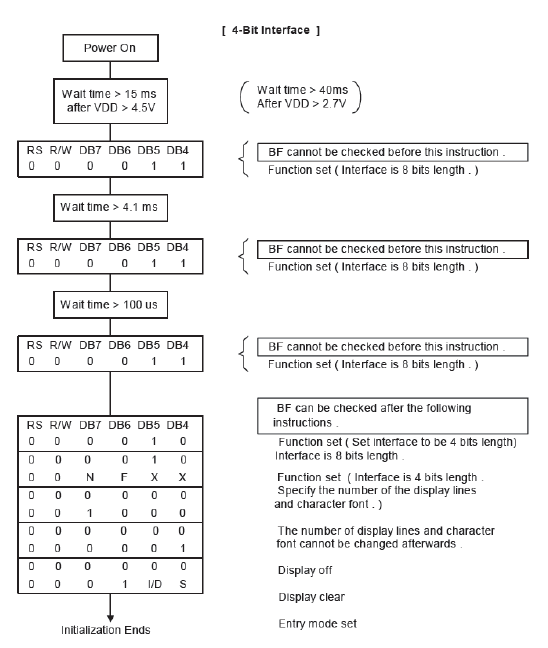
- As you can see the first step (after power on) is to wait more than 40ms after VDD > 2.7V and then more than 15ms after VDD > 4.5V, making 55+ms total before sending any commands to the LCD. Let's round it to 100ms.
- Then we would send command
0x3 - then wait for more than 4.1ms (we'll round it to 10ms)
- then send command
0x3second time, then wait for more than 100us (we'll round it to 1ms) - and send command
0x3for the last time
These steps should be done this way so that the LCD controller complete its reset procedure for further setup. Then the interface setup steps follows after this. Now you must replace your following code:
BANKSEL PORTB
MOVLW 0x03  ;
CALL KOMUTYAZ ;

MOVLW 0x02;
CALL KOMUTYAZ ;
MOVLW 0x28 ;
CALL KOMUTYAZ ;
MOVLW 0x01 ;
CALL KOMUTYAZ ;
MOVLW 0x06;
CALL KOMUTYAZ ;
MOVLW 0x0C ;
CALL KOMUTYAZ ;

MOVLW 0x80;
CALL KOMUTYAZ ;
With the following code:
CALL    Wait100ms   ;< implement this delay
BANKSEL PORTB       ; Make sure your in PORTB bank after returning from the delay
BCF     PORTB,4     ; Set the RS pin low to send command
BCF     PORTB,5     ; Set the Enable pin low
MOVLW   0xF0
ANDWF   PORTB,F     ; Clear Lower 4 bits of PORTB
MOVLW   0x3         ; Load the reset command value
IORWF   PORTB,F     ; Output the command value out of data pins
BSF     PORTB,5
BCF     PORTB,5     ; Generate a falling edge on the Enable pin
CALL    Wait10ms    ;< implement this delay
BANKSEL PORTB       ; Make sure your in PORTB bank after returning from the delay
BSF     PORTB,5
BCF     PORTB,5     ; Latch the 0x3 to the LCD again
CALL    Wait1ms     ;< implement this delay
BANKSEL PORTB       ; Make sure your in PORTB bank after returning from the delay
BSF     PORTB,5
BCF     PORTB,5     ; Latch the 0x3 for the last time
CALL    Wait1ms

; Now setup the LCD interface
BANKSEL PORTB
CLRF    PORTB
MOVLW   2
IORWF   PORTB,F
BSF     PORTB,5
BCF     PORTB,5
CALL    Wait1ms
BANKSEL PORTB
BSF     PORTB,5
BCF     PORTB,5     ; Latch the command value 2 two times
CALL    Wait100us   ;< implement this delay
BANKSEL PORTB
MOVLW   0xF0
ANDWF   PORTB,F     ; Clear the data pins
BSF     PORTB,5
BCF     PORTB,5
CALL    Wait100us
MOVLW   0x8
BANKSEL PORTB
IORWF   PORTB,F
BSF     PORTB,5
BCF     PORTB,5
CALL    Wait100us
MOVLW   0xF0
BANKSEL PORTB
ANDWF   PORTB,F
BSF     PORTB,5
BCF     PORTB,5
CALL    Wait100us
MOVLW   1
BANKSEL PORTB
IORWF   PORTB,F
BSF     PORTB,5
BCF     PORTB,5
CALL    Wait10ms    ; You must delay more than 3ms after sending 0x1 (Clear display command)
MOVLW   0xF0
BANKSEL PORTB
ANDWF   PORTB,F
BSF     PORTB,5
BCF     PORTB,5
MOVLW   6
IORWF   PORTB,F
BSF     PORTB,5
BCF     PORTB,5
CALL    Wait100us
; Finally the LCD should be ready to use with the new interface setup
Make this change in addition to the LVP config. Try and let me know the result.
Upvotes: 0
Related Questions
- PIC18F4580 isn't turning the LED on in Proteus
- Why am I getting this error in proteus: "Invalid opcode 0xFFFF at PC=0x0008"
- Stack overflow in Proteus w/ PIC18F458
- Proteus show characters on LCD ( LM015L )
- PIC LCD Code not running on Proteus 8
- PIC assembly code not working, PICKit2, ultrasonic sensor
- Does proteus support onKey up/down events
- A number to LCD display in assembly in PIC16Fxx
- How to work with Flipkart Proteus Library in Java?
- Used Proteus in an Android Fragment, but getting an error while casting inflater - Proteus Android Layout Engine